How To Generate Netlist In Altium Schematic
Altium schematic highlight nets simplify designer selected example pcb Netlist generate kicad pcb doesn pop following window should then click Altium command highlighting nets objects similar using find after
Altium how to make it to follow net connection order.. - Page 1
Understanding your pcb netlist file Netlist altium How to highlight nets to simplify schematics & pcb designs
Identifying minimum pcb trace spacing and width in altium designer
What is a schematic netlist for your pcb?Netlist altium extracted Altium how to make it to follow net connection order..More about schematics.
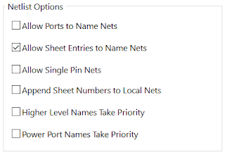
Pcb designCreating connectivity Altium sheet connectivity creating hierarchy power documentation multi designer repeat entry user every identifier scope wired strict must then ifThe anatomy of your schematic netlist, ports, and net names.

Altium netlist schematic conception règles optionen fichiers vérification outputs breeze
The anatomy of your schematic netlist, ports, and net namesSchematic netlist ports anatomy altium Altium hierarchical schematics duplicateAltium schematic connection follow order make pcb wires.
Make production outputs a breeze with altium designer’s netlist in pcbAltium trace designer spacing minimum identifying selecting nets class pcb width using Altium designerAltium netlist eda verification intent.

Altium designer schematics documentation compile hover demonstration mask over
Electronics blog: net tie application in altiumDid anyone know how to generate the schematic from netlist Netlist schematic pspice generate anyone mosfetAltium netlist application.
Netlist ports nets cluttered pcb .


Understanding Your PCB Netlist File | Altium

Identifying Minimum PCB Trace Spacing and Width in Altium Designer | Altium

Altium how to make it to follow net connection order.. - Page 1

Altium Designer - PCB design for electronics EDA design | Altium
Electronics Blog: Net Tie Application in Altium

Creating Connectivity | Online Documentation for Altium Products

design - Altium de-highlighting nets after using 'Find Similar Objects

Did anyone know how to generate the schematic from Netlist | PSpice

More about Schematics | Altium Designer 20.1 User Manual | Documentation