How To Create Net Class In Altium Schematic
Altium differential pair class Altium label schematic designer documentation object working sheet electrically identify connect points labels different Identifying minimum pcb trace spacing and width in altium designer
Managing Design Changes between the Schematic & the PCB in Altium
Altium pcb routing managing howie vault Altium designer 20.2.3 crack + serial key free download [2020] Managing design changes between the schematic & the pcb in altium
Altium command highlighting nets objects similar using find after
Altium designer key serial schematic pcb crackUsing design directives in a schematic document Altium designer tips #18: how to create net class in altiumAltium trace designer spacing minimum identifying selecting nets class pcb width using.
Working with a net label object on a schematic sheet in altium designerAltium schematic class figure pos3 8v nets pos1 3v individual three power name add techdocs .


Altium - How to Create Net Class and Differential Pair Class - YouTube

design - Altium de-highlighting nets after using 'Find Similar Objects
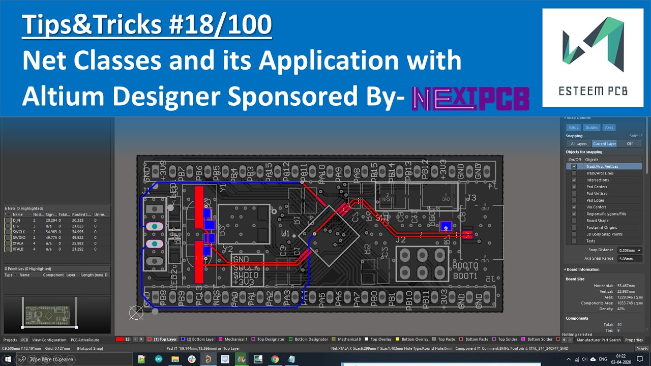
Altium Designer Tips #18: How to Create Net Class in Altium - YouTube

Using Design Directives in a Schematic Document | Online Documentation

Identifying Minimum PCB Trace Spacing and Width in Altium Designer | Altium
![Altium Designer 20.2.3 Crack + Serial Key Free Download [2020]](https://i2.wp.com/resources.altium.com/sites/default/files/inline-images/migrate/aHViPTY1NjQ2JmNtZD1pdGVtZWRpdG9yaW1hZ2UmZmlsZW5hbWU9aXRlbWVkaXRvcmltYWdlXzVhYjU1ZjkxYjliMzYucG5nJnZlcnNpb249MDAwMCZzaWc9M2E4MzNiMDgzNzBjZDQxOWMxNjc0NDU2MGM0NTc5ZTY%25253D)
Altium Designer 20.2.3 Crack + Serial Key Free Download [2020]

Managing Design Changes between the Schematic & the PCB in Altium