How To Update Pcb From Schematic Altium
Altium pcb schematic Altium transferred been Altium designer multi-sheet and multi-channel design [crate sheet
Design pcb schematic and layout in altium by Sociallyvegan
Altium schematics fiverr screen Altium schematic board between designer working documentation ad move functionality reflect feel look How to create a pcb layout from a schematic in altium designer
Altium schematic guideline engineers inflows wiring
Altium pcb layout fiverrHow to create a pcb layout from a schematic in altium designer Updating the pcb from schematic changesClone and modify an arduino mega pcb schematic in altium designer.
Learning pcb design in one weekAltium sheet multi designer symbol channel Pcb altiumAltium arduino pcb conception modify simulatore placas cao logiciel environnement unifié clone.
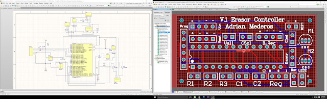
![Clone and Modify an Arduino Mega PCB Schematic in Altium Designer](https://i2.wp.com/resources.altium.com/sites/default/files/doc_import/CpVvvqT6Zj7SQbLH80TnOSAOCyipGt3t9DofXN9e21G0wInBnebK4QLG2fSnOfZGzbljgU5Lc-sZA5L6Us43tW6zjECU3BVs1uEPkFYgYkkzaJoRqb5iLl_xH174Ehl8pk3Hy8Iy.png)
Altium fiverr
Altium pcb pcbs thousandWorking between the schematic and the board Embedded system engineering: altium designer tutorial 4Pcb learning week schematic altium monitors both complete left board.
Pcb altium tutorial schematic update designer document selectAltium pcb schematic screen fiverr Design schematic and pcb in altium by wangdegangPcb design.
![Altium Designer PCB Design Tutorial | PCBCart](https://i2.wp.com/www.pcbcart.com/Uploads/Editor/2016-08-09/57a995846c905.jpg)
Altium pcb
How to create a pcb layout from a schematic in altium designerDesign schematics and pcb in altium by faiz07 A basic guideline from schematic to pcb design for altium designerHow to create a pcb schematic.
Design pcb schematic and layout in altium by sociallyveganAltium designer pcb design tutorial Forbidden placing importing altium schematics unaccessible fallenDesign pcb schematic and layout in altium by sociallyvegan.
![Learning PCB design in one week - We have the Technology](https://3.bp.blogspot.com/-tXDsAiUak0I/V8imfTudvSI/AAAAAAAACuE/Mgq8bAFCavkK8y4AuwFOS22MJbepVNHcwCLcB/s640/boards.jpg)
![How to Create a PCB Schematic | Altium Designer](https://i2.wp.com/resources.altium.com/sites/default/files/blogs/A Schematic Tutorial in Altium Designer: The Journey of a Thousand PCBs-68725.jpg)
How to Create a PCB Schematic | Altium Designer
![Embedded System Engineering: Altium Designer Tutorial 4 - PCB Layout](https://4.bp.blogspot.com/-2pKfZV_-or0/Vny9nzHLP4I/AAAAAAAAA68/x_vFDdi1Opk/s1600/altium_54.jpg)
Embedded System Engineering: Altium Designer Tutorial 4 - PCB Layout
![Design pcb schematic and layout in altium by Sociallyvegan | Fiverr](https://i2.wp.com/fiverr-res.cloudinary.com/images/t_main1,q_auto,f_auto,q_auto,f_auto/gigs/112772182/original/cdf53d2ab648887349485ac23951c0adc512adab/design-pcb-schematic-and-layout-in-altium.jpg)
Design pcb schematic and layout in altium by Sociallyvegan | Fiverr
![Design schematic and pcb in altium by Wangdegang | Fiverr](https://i2.wp.com/fiverr-res.cloudinary.com/images/t_main1,q_auto,f_auto,q_auto,f_auto/gigs/181005974/original/40bd490e13f0e0cf055bfb7f4d3bfdfa958486c7/design-schematic-and-pcb-in-altium.png)
Design schematic and pcb in altium by Wangdegang | Fiverr
![Design schematics and pcb in altium by Faiz07 | Fiverr](https://i2.wp.com/fiverr-res.cloudinary.com/images/t_smartwm/t_main1,q_auto,f_auto,q_auto,f_auto/attachments/delivery/asset/042714782a81a45d93d3005cfceb1748-1595361908/Circuit_bb/design-schematics-in-altium-designer.png)
Design schematics and pcb in altium by Faiz07 | Fiverr
![Working Between the Schematic and the Board | Online Documentation for](https://i2.wp.com/www.altium.com/documentation/sites/default/files/wiki_attachments/296862/AltiumDesigner1.png)
Working Between the Schematic and the Board | Online Documentation for
![A Basic Guideline from Schematic to PCB Design for Altium Designer - RAYPCB](https://i2.wp.com/www.raypcb.com/wp-content/uploads/2021/03/af52d9dac6f02d0-1.png)
A Basic Guideline from Schematic to PCB Design for Altium Designer - RAYPCB
![Design pcb schematic and layout in altium by Sociallyvegan](https://i2.wp.com/fiverr-res.cloudinary.com/images/t_main1,q_auto,f_auto/gigs2/112772182/original/dc3bd3b891d1f9e551c694c9a40367b1722924bd/design-pcb-schematic-and-layout-in-altium.jpg)
Design pcb schematic and layout in altium by Sociallyvegan
![Updating the PCB from Schematic Changes | Altium Designer 17 Essentials](https://i.ytimg.com/vi/QwHGK9ZFjv0/maxresdefault.jpg)
Updating the PCB from Schematic Changes | Altium Designer 17 Essentials