Altium Schematic Template Location
Create a custom altium schematic template Altium template designer schematics Working between the schematic and the board
Create a custom Altium schematic template - PCB 3D
Create a custom altium schematic template Template altium schematic create custom pcb 3d [view 27+] how to draw schematic diagram in altium
Altium generic schematic
Altium tutorialMore about schematics Creating and modifying components in altium schematicsAltium shortcuts.
Altium pcb documentation routing vault migrated supported concordAltium schematic Altium designer schematics documentation compile hover demonstration mask overAltium schematic hackaday io amplifier.

Altium schematic template pcb create custom logo 3d designer delete select
Altium schematicAltium pdf schematic variants Altium trace designer spacing minimum identifying selecting nets class pcb width usingAltium designer getting started user guide & video tutorials.
1 (design the schematic using "altium designer") source: by theAltium designer route hint missing Identifying minimum pcb trace spacing and width in altium designerAltium hint missing route designer.
Altium designer tutorials
Altium researcherStart your schematic with generic components Altium schematic preview.
.


Altium Tutorial - Variants & Printing PDF Schematic - YouTube
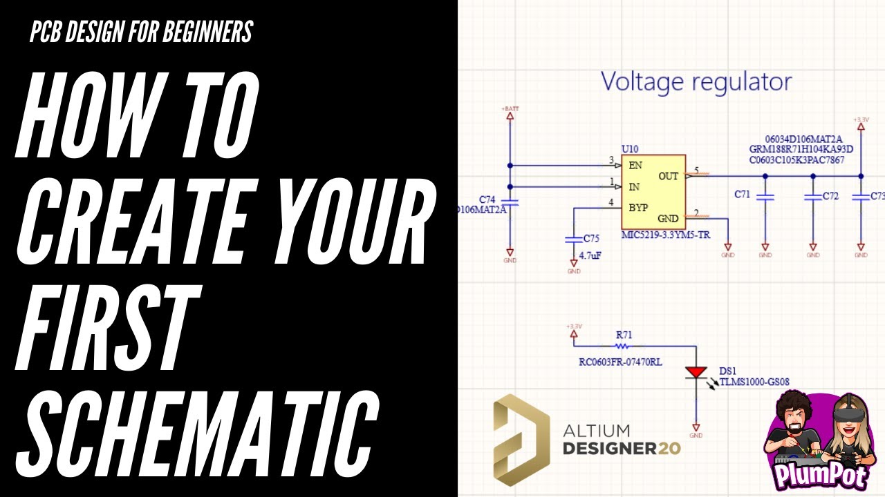
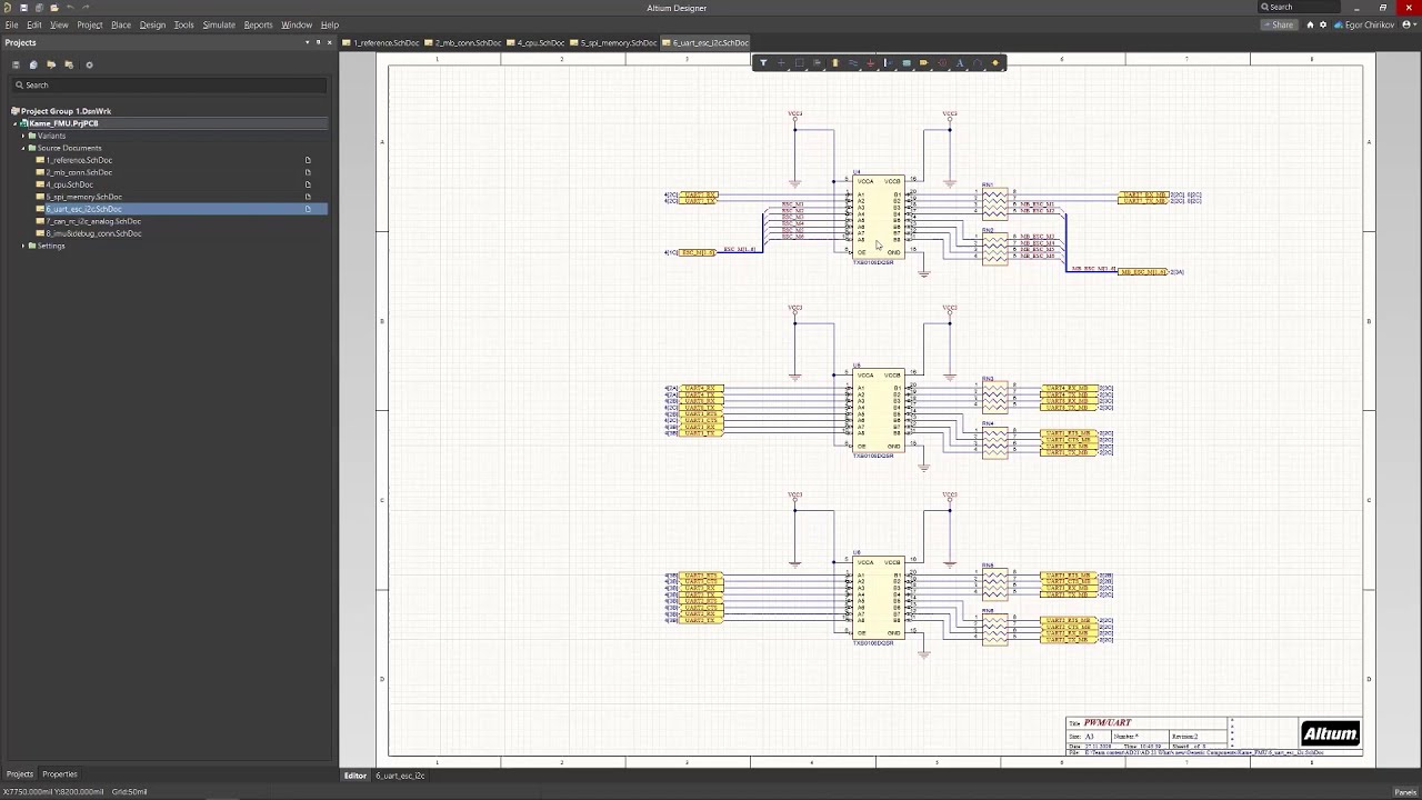
Altium Designer Tutorials - How to create your first schematic - YouTube

schematics - Altium Designer New Template - Electrical Engineering

Identifying Minimum PCB Trace Spacing and Width in Altium Designer | Altium
![[View 27+] How To Draw Schematic Diagram In Altium](https://i2.wp.com/tipsmake.com/data/images/shortcuts-in-altium-most-often-used-picture-2-08rYwkTwB.jpg)
[View 27+] How To Draw Schematic Diagram In Altium

Working Between the Schematic and the Board | Altium Designer 17.1 User

Create a custom Altium schematic template - PCB 3D

Create a custom Altium schematic template - PCB 3D

1 (Design the schematic using "Altium Designer") Source: By the