A Design Schematic Is
Sketching during schematic design Landscaping buildings Schematic site
Schematic Design Package - Alden Miller Interiors
Building design Schematic landscape landscaping true there residential Design considerations for poe
Schematic diagram make coreldraw technical static use try
Schematic drafting paintingvalleySchematic design Schematic sketching during fair enoughWeb site page.
Schematic designSchematic design begins to develop design concepts Schematic bubble diagrams diagram architecture concept concepts site process building starts analysis phase sketch choose boardFpga schematic pcb fig main.
![[Download 34+] Schematic Diagram Architecture Meaning](https://i2.wp.com/www.lifeofanarchitect.com/wp-content/uploads/2014/11/Schematic-Design-13-600x448.jpg?resize=600%2C448)
Poe ethernet surge gigabit considerations
Architectural design studio: my schematic designThere is true: february 2015 Schematic design (part 1)Made in baltimore: architectural design for makerspaces.
Schematic design package[download 34+] schematic diagram architecture meaning Advantages of hierarchical schematic design for pcb schematic layoutsSchematic plan architectural floor makerspaces plans architecture baltimore example makerspace made makezine arriving cbha finer courtesy level scale detail lab.
How to make a schematic diagram in coreldraw
Schematic hierarchical pcb altium advantagesWhat to expect when designing .
.


Schematic Design Package - Alden Miller Interiors

Made in Baltimore: Architectural Design for Makerspaces | Make:
Schematic Design (Part 1) - YouTube

Advantages of Hierarchical Schematic Design for PCB Schematic Layouts

Design considerations for PoE - Electrical Engineering News and Products

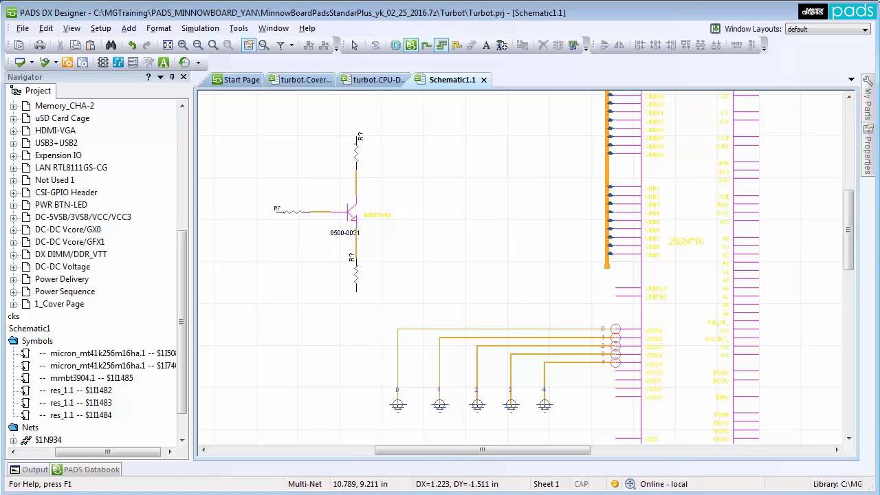
Fig. 1 - Main FPGA schematic page

What To Expect When Designing - Guide

web site page

There is True: February 2015